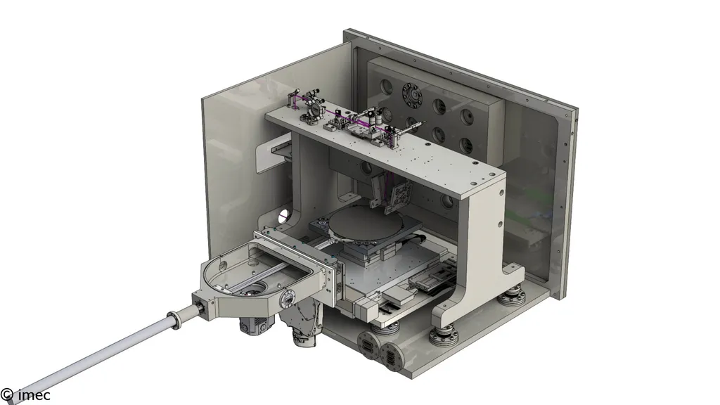
The race to shrink semiconductor nodes just crossed a defining threshold. This week, imec announced a breakthrough in single-patterning high-NA EUV lithography, achieving 20nm pitch line structures with 13nm tip-to-tip dimensions for damascene metallization. Even more remarkable, they demonstrated ruthenium lines at 20nm and 18nm pitch using a direct metal etch (DME) process, with a 100% electrical test yield for the 20nm pitch structures. Presented at the 2025 SPIE Photomask Technology + EUV Lithography Conference, these results mark a critical step toward enabling sub-2nm logic nodes—an advancement with profound implications for audio processing chips, where power efficiency and signal integrity are paramount.
For audio hardware engineers, the significance lies in the ability to pack more transistors into a given area without sacrificing performance or increasing power consumption. Traditional EUV lithography struggled to maintain yield and reliability at such fine pitches, especially for analog and mixed-signal circuits that underpin high-fidelity audio processing. The use of ruthenium—a metal known for its resistance to electromigration and compatibility with advanced interconnects—addresses longstanding reliability issues in high-density audio DSPs and ADC/DAC interfaces. “The 100% electrical test yield for these structures is a game-changer,” noted an imec spokesperson. “It proves that high-NA EUV can deliver the precision and repeatability required for next-generation audio and RF applications.”
This breakthrough also challenges the status quo in chip design workflows. Until now, achieving sub-20nm features often required complex multi-patterning schemes, which increased cost and design cycle times. The new single-patterning approach not only simplifies the process but also opens the door for more aggressive scaling in analog and RF circuits—areas where multi-patterning was particularly cumbersome. For audio professionals, this means faster iteration cycles and the potential for more sophisticated on-chip signal processing, such as real-time spatial audio rendering or ultra-low-latency effects processing, without the thermal or power penalties of previous generations.
The broader impact extends beyond chip density. As the industry moves toward sub-2nm nodes, the integration of advanced materials like ruthenium and the refinement of high-NA EUV processes will enable audio hardware designers to push the boundaries of performance and efficiency. This could accelerate the development of ultra-compact, high-channel-count audio interfaces, immersive audio processors, and even new classes of smart transducers that leverage on-chip intelligence. For an industry where every decibel of dynamic range and microsecond of latency matters, imec’s milestone is more than a manufacturing win—it’s a clarion call for audio engineers to reimagine what’s possible at the silicon level.
**Sources:**
* https://semiengineering.com/chip-industry-week-in-review-105/
* https://semiengineering.com/chip-industry-week-in-review-105/
* https://semiengineering.com/chip-industry-week-in-review-105/

